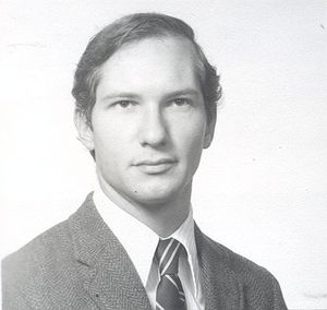
Lawrence H. Goldstein
- Birthdate
- 1952/01/07
- Associated organizations
- INMOS Corporation
- Fields of study
- VLSI
- Awards
- IEEE Browder J. Thompson Memorial Prize Paper Award
Biography
Lawrence H. Goldstein was born in New York, NY, on January 7, 1952. He received the B.E. degree in Electrical Engineering from The Cooper Union School of Engineering and Science, New York, NY, in 1973. He was granted the M.S.E., M.A., and Ph.D. degrees from Princeton University, Princeton, NJ in 1974, 1975, and 1976, respectively, all in electrical engineering.
From 1976 through April 1980, he was a Member of Technical Staff in the Computer-Aided Design Division of the Integrated Circuit Design Department at Sandia National Laboratories in Albuquerque, NM. While at Sandia, he worked in the areas of photovoltaic system simulation and testability analysis of digital circuits. He joined INMOS Corporation in Colorado Springs, Colorado in May 1980 as a Senior CAD Engineer. His major responsibilities at INMOS include circuit and timing simulator development and CAD systems for VLSI memory design.
Dr. Goldstein, a member of the Institute of Electrical and Electronics Engineers, is a member of Tau Beta Pi, Eta Kappa Nu, and is editor of the ACM SIGDA Newsletter.
