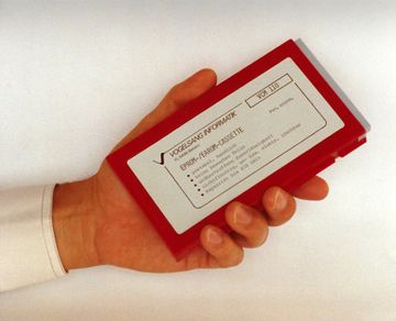
First-Hand:EPROM Cassette (1977) as a Predecessor of the USB Flash Drive
contributed by Remo J. Vogelsang, IEEE Life Member, President/Owner Remo Vogelsang AG Engineering Informatik from 1974 to 2015
Fitting technical information is available by clicking the [index] ![]() . Please click Smiley's
. Please click Smiley's ![]() [index] for background information or maybe a funny tale ! To return click ↑.
[index] for background information or maybe a funny tale ! To return click ↑.
Evolution of Pluggable Memory Devices
Ubiquitous - from a few kilobytes to terabytes
Conceived already in 1977 and produced from 1979 till 1988 the Memory Cassette stands at the very beginning of the evolution of the pluggable and portable semiconductor memory devices. Products of comparable characteristics got commercially available only around 1990 - apart from a sales attempt made on a magnetic storage solution. Called Memory Card, Memory Stick, USB Flash Drive, Flash Drive, USB Stick - or known under a variety of other names - they still carry the same distinctive features as their forerunners, except for their tremendous capacity-size-price advantages, made possible by the incredible progression in semiconductor manufacturing. This historical succession represents a notable, most comprehensible example, illustrating the evolution predicted by Moore's Law:
A more than ten-million-fold capacity increase (64 KB to 640 GB) at a one-hundred-fold space decrease (240 cm³ to 2.4 cm³), resulting in a more than one-billion-fold capacity to size augmentation, taking place within 35 years, all with the benefit of a 10-million-fold cost decrease ($ 4.00 per KB to $ 0.40 per GB).
Features These more and more appreciated and popular devices were gradually aligning to the available technology in parallel with the rising expectations of their users, still retaining their ever valid core attributes:
- Detachable and portable
- Non-volatile
- Ruggedness (no harm by surface scratches)
- Durable and reliable, no moving parts.
- Immune to electromagnetic interference (unlike floppy disks)
- Field-programmability
- Single supply voltage
- Hot swapping possible
- Tailored capacity range
- Opportune interface
Exploding Evolution It started as a sort of a convenient template for reliably handling machining data under rough environmental conditions, replacing cumbersome paper tapes (punched tape) or avoiding flimsy floppy disks spinning in bulky peripheral drives. On the system level, it perfectly fitted the prevailing 8-bit and 16-bit microprocessor platforms. Over the years, gaining in capacity while shrinking in size, the pluggable memory progressed towards the now ubiquitous data storage devices, suitable for all sorts of applications, with possible storage capacities beyond anybody's expectations.
|
|
|
|
|
| Memory Cassette | Bubble Memory Cartridge | Memory / Flash Card | USB Flash Drives | Type |
|---|---|---|---|---|
| 1980 | 1981 | 1990 | 1998 | Phase-in |
| 4 to 56 KB | 8 to 32 KB | 64 KB to 240 GB | 128 MB to > 1 TB | Capacity Range |
| 160 x 100 x 15 mm | 60 x 45 x 20 mm | 32 x 24 x 2.1 mm (sample) | 40 x 12 x 5 mm (sample) | Approx. Size |
| memory standard | proprietary | several | USB | Interface |
| none | none | several | USB mass storage | Standard |
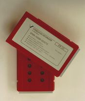
- Memory Cassette: Designed in the then popular Eurocard format, it featured all necessary attributes enabling the use of a succession in technology ranging from EPROM to EAROM to EEPROM to BBSRAM. Initially designed as EPROM/EAROM-Cassette, it contained from 4KB to 56KB of Erasable Programmable Read Only Memory.
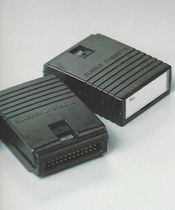
- Bubble Memory Cartridge: Fujitsu Limited launched the 'Bubble Memory Cartridge' targeting an applications range similar to the one covered by the 'Memory Cassette'. The applied technology was based on using a thin film of a magnetic material to hold small magnetized areas - known as bubbles - as information storage. But it never became a serious contender against the steadily progressing market of non-volatile semiconductor memories. The cartridge could not be mounted like a printed circuit card into a card magazine, but required instead a special mounting socket. Applying it required the expenditure of a peripheral device.
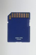
- Memory Card or Flash Card: Designed in many different formats, sizes, interfaces and standards to cover the markets for cell-phones, digital cameras, industrial applications, etc., mounting is typically in a concealed fashion, fitting enclosures of the specific device. The technology used is based on the flash memory, the yet unchallenged, modern offspring of the EEPROM. A specialized version known as the SIM Card (Subscriber Identity Module) is used in mobile phones. Its functionally independent size ranges from a credit card to a small plate of 6x5 mm (for embedded-SIM). The meanwhile almost obsolete, credit card-sized PC Card was initially conceived as a memory device. It soon morphed to a series of popular peripheral interfaces, designed for laptop computers. It is still used as conditional-access module in television equipment.
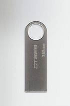
- USB Flash Drives: The technology of this ubiquitous storage media of the day - mounted in the typically protruding stick-fashion - is also based on the flash memory. Apart from the clever choice of the Universal Serial Bus (USB) as the interface, the unique form of its connector - what a lucky strike - facilitates all sorts of form factors.
EPROM/EAROM Cassette
What a neat, novel, elaborate, handy gadget
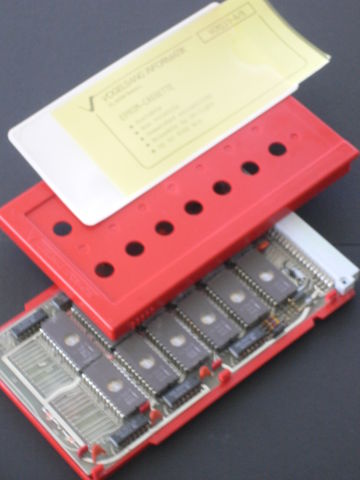
Bottom half with embedded printed circuit board, assembled with 12 EPROM devices, protection diode arrays and additional interface circuitry.
Top half containing openings, admitting exposure to ultraviolet light for erasure.
Adhesive foil used for closing the openings in the unit as well as for its labeling. Shown is a fitting translucent labeling pocket with the inserted tag.
The Memory Cassette was built as a plug-in unit including a printed circuit board and an injection-molded housing comprising two halves. The housing had ribs (with latch notches) on its narrow sides, which were aligned with the printed circuit card. The unit was outfitted with a connector according to DIN 41612 with 2 x 32 contacts, fitting 0.1 inch (2.54 mm) grid pitch. As a whole - encasement inclusive - it was conforming to the norm of the Eurocard (printed circuit board) format of 160 x 100 x 15 mm, a most popular size at the time. Fitting into standard IEC 60297 racks, it was therefore facilitating the integration into given equipment.
Description
The printed circuit board included two to fourteen semiconductor memory devices, a number of protection diode arrays, some necessary interface circuits and the connector. Inserted into the bottom half of the housing with its ribs, together they formed the 160 x 100 mm standard card size. The top half of the housing contained openings at locations corresponding to the quartz windows of the underlying memory devices, admitting - where applicable - exposure to an ultraviolet light source. Both halves of the housing were kept together by six resilient tabs, which were engaging when both halves of the housing got pressed together. Due to the solvable plastic material used, it was possible to make a permanent connection if the resilient tabs were wetted with solvent. The bottom half of he housing was fitted with a recess for posting an adhesive type plate. A suitable recess was also made to the top half, in order to facilitate the positioning of the adhesive foils used for closing the openings on the cover, as well as for appropriate labeling.
Originally, the VMC110-A/B Cassette was planned to contain from 4KB to 56KB of Erasable Programmable Read Only Memory (EPROM). However - in anticipation of further development - it was designed such, that its printed circuit board may also have got equipped with other types of memory devices, like EAROM, EEPROM, BBSRAM. Read access may have taken place at full memory speed for any of the device type. To exclude damage due to static discharge, special protection was provided to the relevant signal terminals. Provisions were made, that allowed cassettes to get interchanged without power interruption and ensuring proper cassette insertion. Necessary circuits for status check under program control were provided, allowing the detection of specific cassette types. Programming of any of the cassette types was done electrically via the appropriate function terminals. Operation required a single 5V supply only (except for programming). A UV-lamp, supplemented with a fitting tray, allowed erasing the entire data contents of the cassette at once.
The interface used was fully based on the access and control architecture of the then prevailing 24-pin semiconductor memory devices, which were known to any designer using the 8-bit and 16-bit microprocessor platforms. This turned out to be advantageous for using the Cassette Memory in various systems. Then our supplementary development set, containing hardware- software- and assembly elements, also provided valuable support. For the whole family of PDP-11/03TM and LSI-11TM microprocessor systems, we had a full set of mature, well-engineered, proprietary products for interfacing, programming, assembling and maintenance at our disposal.
Cassette Products
| Type | Capacity | Memory Technology | Storage Devices | Programming |
|---|---|---|---|---|
| VCM 110-A |
4 … 28 KB | EPROM erasable programmable read-only memory | (2Kx8) |
UV erasable / electr. progr. |
| VCM 110-B |
8 … 56 KB | EPROM erasable programmable read-only memory | (4Kx8) |
UV erasable / electr. progr. |
| VCM 110-C | 4 … 28 KB | EEPROM electrically erasable progr. read-only memory | (2Kx8) |
electr. erasable and progr. |
| VCR 110-A | 4 … 28 KB | BBSRAM battery-backed random-access memory | (2Kx8) |
regular random-access write |
Are you somewhat confused about EAROM / EEPROM / FLASH memory? No surprise. ![]() [tale 1]
[tale 1]
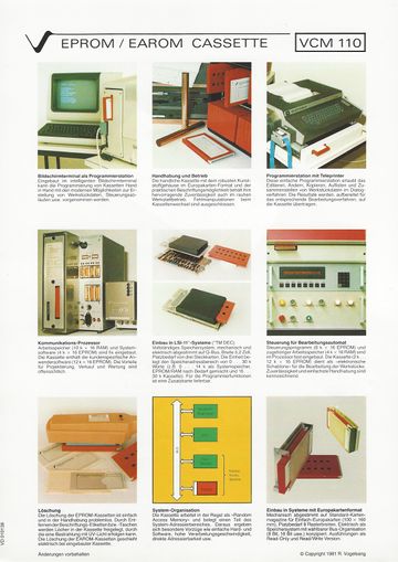
from top-left to bottom-right
- Intelligent Terminal Programming Station
- Handling and Operation
- Teleprinter Programmiing Station
- Communication Processor
- Integration into LSI-11 Systems:
- Numerical Control System
- Erasing by UV-light Exposure
- System Scheme
- Integration into Euro-Card systems
Application
- The classic: To reliably handle template-like machining data in numerical control systems, sample data in testing equipment, collect data in data loggers under rough environmental conditions commonplace in machine shops or on outdoor sites.
- Storage of application and/or customer oriented program and data portions in so-called embedded systems - often operating under real-time computing constraints - with dedicated functions within a larger electrical or mechanical system. Here field-programmability was a very desirable feature, as it could reduce turnaround time and cost for exchanging modified firmware.
- Any application requiring portable memory under severe environmental and handling conditions.
- Simplifying servicing and repair work (in case of presumed or real fault) by allowing the exchange of firmware by unskilled personnel.
System-Information
- In true read-only applications - i.e. a programmed cassette served as a data source - interfacing was simply done through galvanic connections between the appropriate terminals of the cassette and the microprocessor memory bus. No additional electric components, such as line drivers/receivers, were needed. The interfacing task was reduced to arranging a clever mechanic connecting scheme.
- For off-line programming - i.e. data programming of the cassette was done externally from the target equipment or a dedicated programming station - any brand of those off-the-shelf EPROM programmers construed to program one single memory chip at a time (almost everybody had one like that at his disposal), was good enough. Provided one afforded undergoing all those laborious programming procedures necessary. A simple gadget made of fitting connectors, a rotary switch and some wiring was required as a supplement.
- Equipment, such as a data logger or a cassette programming station, which absolutely required built-in programming facilities, needed a dedicated, built-in programming module with adequate data access to whatever source required.
- As mentioned before, there existed a whole set of hardware and firmware to efficiently merge the cassette system with the family of PDP-11/03TM and LSI-11TM microprocessor systems: a) The EPROM/RAM memory system VMC11-A which may have contained up to 32 KB/(28 KB) of EPROM and/or RAM, also providing all the electrical and mechanical means to readily interface to the VCM110-A/(B) EPROM Cassettes. b) The EPROM-Programmer VMP11-A, an option enabling programming of the VCM110-A/(B) EPROM Cassettes as well as the EPROM/RAM memory system VMC11-A.
Development
Seize the chance
Particular requirements of a customer of mine initiated the development of this pluggable memory. For his planned custom machine-tool he needed a numerical control (NC, CNC) with properties beyond the capabilities of common, off-the-shelf solutions available at that time. He also expected some appropriate device - sort of a template - for handling machining data reliably under the rough environmental conditions prevailing in his machine shops. He was very reluctant, if not defiant in accepting paper tape (punched tape) or floppy disk (8-inch and 5¼-inch emerging on the market then). He had strong arguments for sure, although fitting solutions did not exist yet. However, he signaled to provide adequate compensation for following through his viewpoint. ![]() [tale 2]
[tale 2]
Conception
It was spring 1977. The notion of the pluggable memory took form on a hastily jotted sketch during the train ride home from an inspiring meeting with this customer, located in the western (French speaking) part of Switzerland. It showed a number of EPROMs, placed on a fittingly encased printed circuit board, the size of the then widely utilized Eurocard. Openings, placed in the encasement at corresponding locations to the quartz windows of the underlying EPROM-devices, allowed exposure to ultraviolet light for erasure. Finally, a removable label holder, normally covering these holes, carried the identification.
Choosing a practical interface was as crucial as it was simple - regarding the prevailing context. Its characteristics are best understood by consulting the description in the [2716] ![]() EPROM datasheet. At that time, developers were familiar with the simple scheme: Read-access required eleven input signals to select the address of the particular cell, eight multiplexed outputs to read its content and one control signal to select the memory device. One additional input was available to control programming (write). By suitably arranging these signal lines, supplementing them by appropriate power lines and fitting cassette identification signals and by properly protecting connections against damage by electrostatic discharge, an unpretentious, well defined, widely acceptable interface got created - avoiding red tape.
EPROM datasheet. At that time, developers were familiar with the simple scheme: Read-access required eleven input signals to select the address of the particular cell, eight multiplexed outputs to read its content and one control signal to select the memory device. One additional input was available to control programming (write). By suitably arranging these signal lines, supplementing them by appropriate power lines and fitting cassette identification signals and by properly protecting connections against damage by electrostatic discharge, an unpretentious, well defined, widely acceptable interface got created - avoiding red tape.
Design and Implementation
Already in mid 1976 we had developed our own Q-bus compatible 8 KB EPROM Memory Card [VME11-A] ![]() , based on the then popular 1K x 8 EPROM circuit [2758]
, based on the then popular 1K x 8 EPROM circuit [2758] ![]() , in conjunction with an appropriate Programmer Card [VMP11-A]
, in conjunction with an appropriate Programmer Card [VMP11-A] ![]() , to be able to accomplish our goals in projects based on PDP-11/03TM and LSI-11TM microprocessor platforms.
, to be able to accomplish our goals in projects based on PDP-11/03TM and LSI-11TM microprocessor platforms. ![]() [tale 3]
[tale 3]
Meanwhile - in order to fulfill rising demands and to keep up with progress in memory technology - the development of the 32 KB Memory Card [VMC11-A] ![]() , based on the newly available 2K x 8 EPROM circuit [2716]
, based on the newly available 2K x 8 EPROM circuit [2716] ![]() got under way, featuring four-fold capacity and versatile usability. One such card covered 32 KB, one half of the intrinsic memory space (16-bit address) of the LSI-11, also allowing to freely mixing EPROM with SRAM in 4 KB segments. Anticipating the emergence of electrically erasable PROM[1][2] - fitting EEPROM did not exist on the market yet - we included necessary functions, allowing to switch among EPROM and EEPROM.
got under way, featuring four-fold capacity and versatile usability. One such card covered 32 KB, one half of the intrinsic memory space (16-bit address) of the LSI-11, also allowing to freely mixing EPROM with SRAM in 4 KB segments. Anticipating the emergence of electrically erasable PROM[1][2] - fitting EEPROM did not exist on the market yet - we included necessary functions, allowing to switch among EPROM and EEPROM.
The availability of this innovative set of mature, well-engineered, proprietary memory products, in conjunction with our proficient team in designing, prototyping and debugging such devices, had unintentionally propelled us into an advantageous position to jump-start this cassette project and to implement it efficiently and successfully. Development efforts and costs remained on a limited scale, since interfacing to the cassette is simply done through galvanic connections between the appropriate terminals of the cassette and the internal memory bus of the Memory Card. So the interfacing task boiled down to arranging a clever mechanic connecting scheme. Then, the providently designed Programmer Card - using the features of the LSI-11 On-line Debugging Tool (ODT) - needed only a few minor extensions at the firmware level to serve the additional requirements. Refraining from a compromise using some sort of a makeshift cover, I decided for the professionally produced, injection-molded plastic encasement, which required an expensive tool and a long lead time.
Conceived during spring 1977 and the customer's order coming in towards the end of 1977, we had completed the cassette design in the middle of 1978. Since fall 1978 the cassette system was operational in several ongoing projects (using makeshift encasements). We had postponed the design release of the encasement for as long as possible to ascertain that no detail got overlooked; early 1980 the first regular batch was produced.
Marketing and Patent Issues
Never knew a prospector yet that died rich[3]
Marketing Efforts Engineering was our business model - not production. So it was ok to design and manufacture technically attractive components - such as modules - on a small scale. In other words we would pick opportunities to rapidly close certain demand gaps. After a couple of years, when the applications technology had jumped to these novel opportunities, we would abandon such products. However, the cassette product offered qualities, worth to consider a longer term commitment. Fact was, the proliferation of solid-state memory with its incessant increase of capacity, the emergence of the EEPROM - a predecessor of flash memory, combined with the eventual prospering of the surface-mount technology (SMT) would pave the way for a vast market of portable solid-state memory. The launching of the 'Bubble Memory Cartridge' by Fujitsu Limited in 1981 - targeting an applications range similar to the one covered by the 'Memory Cassette' - raised hope, that we could profit from their advertising such memory products. Confident about our product, we were looking forward to compete. But soon, Fujitsu's initially impressive promotion ceased.
Right during conception of the cassette, I became aware, that it might make sense to up the stakes in this case and to venture for a marketing trial. However, having never underestimated what it takes, to market a novel product, I was cautious not to squander our resources. We constrained such efforts to a modest promotion, periodically distributing [leaflets] ![]() and void Cassette [specimen]
and void Cassette [specimen] ![]() . Over the years (until about 1988), a fair quantity of cassettes and cassette systems got manufactured to cover our own requirements and to supply our regular customer base. The cassette system proved to be of extraordinary reliability and versatility, to the benefit of many applications.
. Over the years (until about 1988), a fair quantity of cassettes and cassette systems got manufactured to cover our own requirements and to supply our regular customer base. The cassette system proved to be of extraordinary reliability and versatility, to the benefit of many applications.
Patent Applications
Realizing, that aiming to exploit a presumably vast market of portable solid-state memory would be too big a world, I considered it advisable, to at least apply for patents, thereby preserving the rights for possible licensing. Due to pertinent experiences, I was cautiously optimistic regarding patent procedures and feasible benefits. I was mindful too, that besides the USA also Japan would become of great importance. Buying and using EPROMS in respectable quantities over a number of years - it turned out, that US manufacturers adhered to standards of acceptable quality limit (AQL), not suitable for dense semiconductor circuits. Customers had to carry the burden of intolerable quality losses. Apparently aware of this handicap, the emerging Japanese producers were shipping zero defects (ZD) parts - therefore rapidly gaining market share. Eventually I applied for patents in four countries:
| Country | Appl. Date | Appl. Nr. | Patent Nr. | Status |
|---|---|---|---|---|
| Switzerland | 22.09.1980 | 7 083/80-4 | first response 14.01.1985, abandoned | |
| Germany | 04.11.1980 | P 30 41 596.4 | DE 30 41 596 C 2[4] | granted 15.12.1983 |
| USA | 14.09.1981 | S.N. 301,859 | fruitless, abandoned | |
| Japan | 22.09.1981 | 148932/'81 | no official response, abandoned |
The patent procedures went on at a sluggish pace. ![]() [tale 4]
The results, after long waiting times, were meager. Extending expedient efforts - i.e. diligently instructing examiners - would have become prohibitive. Worse, considering tardy patent procedures versus the speed of change in the semiconductor field, the cassette in its original form would have soon become outdated. I decided to abandon this path. You can't win them all!
[tale 4]
The results, after long waiting times, were meager. Extending expedient efforts - i.e. diligently instructing examiners - would have become prohibitive. Worse, considering tardy patent procedures versus the speed of change in the semiconductor field, the cassette in its original form would have soon become outdated. I decided to abandon this path. You can't win them all!
Round-Up
What will be, will be
For us doing engineering, the goal is to successfully fulfill an urgent demand by efficiently applying current and near future technology, avoiding red tape. Usually there is little time left for contemplating circumstances. In retrospect, I am trying to make a fair assessment of work done and of historical facts:
- What began in 1977 on a limited scale for special purpose applications, had developed - not to say exploded - to become a ubiquitous article of daily use, produced in gigantic numbers.
- For sure, the Memory Cassette was a first portable memory. It took years until a comparable follow-up emerged. Due to the almost non-existent marketing, its perception was undervalued.
- Patent attorneys and examiners were struggling to appreciate the intrinsic idea. At that time - personal computers were years away - few people were knowledgeable about computer technology. It appears that the appraisal of the mechanical aspects of the cassette prevailed. Patent efforts and money spent returned no apparent benefit.
- This story may serve as a fitting example to highlight Moore's prediction, written in his seminal 1965 paper.
- Right now, it feels that memory sticks are small enough, and that their capacity is abundant; but then, how many times did we fool ourselves, predicting saturation regarding bulk memory! Let the expert speak: "… It eventually saturates out. I guess I see Moore's Law dying here in the next decade or so, but that's not surprising." - from Gordon Moore in an interview, published in IEEE Spectrum's April 2015 issue's Special Report '50 Years of MOORE'S LAW'[5]
References
To get to the bottom of things ….
- ↑ Patent US4114914: "Electrically Erasable Semiconductor Memory", filed on Feb. 22, 1977, published Sep. 26, 1978, inventor Elijahou Harari.
- ↑ ETHW-Milestones: The Floating Gate EEPROM, 1976 - 1978
- ↑ Quote from B. Traven's: The Treasure of the Sierra Madre
- ↑ "Patent DE3041596 C2: "Steckeinheit mit Steckkarte und Vielfachstecker", filed on Nov. 4, 1980, published Dec. 15, 1983, priority date: Sept. 22, 1980, inventor Remo Vogelsang. [patent]

- ↑ Rachel Courtland: The LAW That's NOT A LAW, IEEE Spectrum, April 2015, No.04.15, pp. 36-38, 56,57
Behind the Scenes
Tales, some serious some funny !
- ↑
 W_h_a_t__F_l_a_v_o_r___P_l_e_a_s_e_?___________________ For somebody who did not have a chance to witness the history of the development of these non-volatile memory devices, some of the distinctions among EPROM, EAROM, EEPROM and Flash might appear incomprehensible at first glance. A few explanations may be helpful. First, the storage principles of all the types are based on a similar semiconductor structure. The functional core distinctions are as follows:
EPROM Erasable programmable read-only memory Access is byte-wise for data read and electrical programming. Erasure is only possible as a whole by using ultraviolet light.
EAROM Electrically alterable programmable read-only memory Access is bit-wise for data read, as well as for electrical erasure and programming.
EEPROM Electrically erasable programmable read-only memory Access is byte-wise for data read, as well as for electrical erasure and programming.
Flash Flash memory Access is block-wise for data read, as well as for electrical erasure and programming.
Finally, let's consider several important characteristics like read access and programming speed, programming voltage, endurance, efficient use of silicon chip area, production technology, etc. Elaborate information, also considering the historical context, are provided within the article Read-only memory describing this storage medium class as a whole. In the comparison Flash memory versus EEPROM additional insight is given regarding flash - the modern type of EEPROM; it explains for instance, that flash is in some sense a step back functionally, since access and erasure can only take place in large chunks. With The difference between EEPROM and Flash another coherent description is on hand. - ↑
 P_r_o_j_e_c_t___D_e_s_i_g_n___b_y___S_q_u_a_b_b_l_i_n_g___ Preferably, I would adapt to the
prevailing meeting style of a customer - myself keeping a low profile, listening, taking notes, checking progress against my own agenda, asking questions, letting meeting members explain, sometimes trying to unblock a muddled situation. Thereby I could gain most genuine opinions, rich information as well as consent and trust. Towards the end of a meeting, after most issues were exhaustively discussed, I would bring up missing items corresponding to my agenda. The few of my own preferences and needs still open, would usually meet little resistance, if any at all. As a result, closing in consent was the rule. However, the proceedings of this meeting deserve extra mention. The CEO/owner of this company had sent me a handwritten, sort of a specification in advance, of some new production equipment to be developed and built. This was very useful for me, getting to know the conceptual ideas the client had developed, allowing a focused preparation for the upcoming design meeting. Also attending such meeting was the head of production engineering. He was in charge of development and implementation of all special machine-tools. He would enter the discussion by ruffling up most arguments his boss had presented - in a restrained demeanor, nevertheless provoking hefty challenges. Soon the discussion would heat up, escalating in volume and repeatedly through acerbic comments - what a battle of two most dedicated problem solvers! So many important details, crucial conditions and vital experiences got spilled out, that I got overwhelmed with plenty of very useful information. Taking notes, sometimes asking questions, I got well prepared to bring about a tangible proposal - hopefully enriched with some innovative details to bridge apparent gaps, made visible by the two antagonists. At noon - agenda closed - it seemed that the morning had ended in an almost irreparable discord among the two men. Together we left for lunch to a chalet in bucolic surroundings, not uncommon of the alpine region. Enjoying a fine meal, discussing private things, doing small talk, we spent lunch in a most pleasurable mood. Back again at the company, in a concise debriefing before parting, we fixed how to proceed. In the years to follow, when I got the chance to participate in other projects of this remarkable company, I repeatedly had the pleasure to experience this fruitful pattern of doing meetings.
- ↑
 F_r_o_m___S_i_m_p_l_i_s_t_i_c___t_o___S_i_m_p_l_e_________ It began with small microprocessor based - more often embedded - control solutions, often requiring only a single package of EPROM (with one piece EPROM prices still in the 100$-range). Updating a program was somewhat cumbersome. It was common procedure to remove every single chip from its module, erase it under a UV-lamp, reprogram it using a single-slot EPROM-programming equipment, relabel it correctly and finally insert it back to the appropriate socket (an extra cost factor) on the module. What was adequate for special purpose, small microprocessor solutions, requiring one or only a few EPROM devices, got to become a nuisance and a prohibitive procedure when whole arrays of EPROM had to get served.
Among all the suppliers of microprocessor chips and/or systems, DEC came up first with the so called On-line Debugging Tool (ODT). Halting the program, the dual mode processor would switch from run to debugging mode, immediately enabling the built in debugging tools (firmware). The inconvenient, quite expensive, microprocessor development system (usually a large box before getting resized to a printed circuit board) became dispensable.
Equipped with the best of the system prerequisites, DEC still missed the chance to come up with an appropriately innovative solution, when first including EPROM devices into their module portfolio. With their MRV11-BA EPROM/RAM (4kx16/256x16) design, they hit the lowest standard possible. Not even a straightforward (almost no cost) connection scheme got considered, to at least enable 'on board programming' through some makeshift means or some dedicated user's tool. Dependent on EPROM-based memories for our ongoing PDP-11/03 / LSI-11 based projects, and considering our being responsible for maintenance and support for years, we could not afford such a simplistic solution, prone to possibly thwart the appreciation of our customers. Relying on our team's proficiency in designing such devices, I decided to build the Memory Card [VME11-A] and an appropriate Programmer Card [VMP11-A]
  . Within four months we had a set of preproduction modules running.
- ↑
 "T_h_e___S_l_e_e_p___o_f___t_h_e___J_u_s_t_______________" Getting a patent granted can become a tricky business, not least considering the different rules in different countries. Obstacles can become adamant - even for powerful companies - as illustrated in the paragraph Role of Patents by the author of an article about LCD development. Evidently fairly simple objects such as the cassette were prone to cause considerable troubles. Some of the patent attorneys and examiners - notably more mechanically oriented and probably lacking expedient interdisciplinary knowledge - did hardly envision the usefulness of such portable memory. Neither were they sufficiently acquainted with the incredibly progressing semiconductor memory technology.
S w i t z e r l a n d : Unbelievable, the Swiss Patent Office stole the show. It took them four years (22.09.80 - 11.10.84) to figure out, what objections could probably be raised against the application, lacking a concise appraisal - what a joke!
G e r m a n y : The patent got granted within a reasonable timeframe. No effective objections against it were raised. In a previous consultation, suggested by the examiner, we got the opportunity to thoroughly treat all aspects of this issue.
U S A : After two years of pondering, the prospect for a positive outcome was still there, but substantial instructing efforts would have been required to go on. According to the various exchanges among attorney and examiner it was to assume, that due care and diligence was not given as needed. The attorney of the renowned law office treating the case wrote: 'It appears to us that the examiner has not done his homework in this case and might be embarrassed if we were to take an appeal' (08.07.83).
J a p a n : There was never an acknowledgement from the Patent Office regarding our patent application. What a simple method to hide or thwart something: A behavior bordering upon deceit.
Copyright © 2015 by Remo Vogelsang
